Difference between revisions of "Wireless Affective Devices"
PaoloVilla (Talk | contribs) |
PaoloVilla (Talk | contribs) |
||
| Line 234: | Line 234: | ||
To guarante maximum flexibility an further update, board provides both ICD and JTAG connections (allowing on-board programming and debugging) through a couple of indipendent dedicated connectors fully compatibles with Microchip programmers and evaluation boards. | To guarante maximum flexibility an further update, board provides both ICD and JTAG connections (allowing on-board programming and debugging) through a couple of indipendent dedicated connectors fully compatibles with Microchip programmers and evaluation boards. | ||
| − | [[Image: | + | [[Image:WADMicro.jpg]] |
=== '''Wireless Connection''' === | === '''Wireless Connection''' === | ||
Revision as of 11:53, 12 December 2009
Wireless Affective Devices
| |
| Coordinator: | |
| Tutor: | SimoneTognetti (tognetti@elet.polimi.it), MatteoMatteucci (matteo.matteucci@polimi.it) |
| Collaborator: | |
| Students: | PaoloVilla (paolovilla79@gmail.com) |
| Research Area: | BioSignal Analysis |
| Research Topic: | Affective Computing |
| Start: | 2008/01/08 |
| End: | 2009/12/30 |
| Status: | Active |
| Level: | Ms |
| Type: | Thesis |
Contents
Project aims
”Everyone knows what an emotion is, until asked to give a definition”

                                                                Beverly Fehr and James Russell
Research on Human-Computer-Interfaces has recently begun to take into account the affective state of the user. By appropriately reacting to the affective user state, interfaces could not only become more pleasant or entertaining, but also more effective or safer. It is known that affective states have bodily correlates, and thus physiological signals could provide the necessary information for acquiring the affective user state. In contrast to other sources of information about the affective user state such as speech or facial expression, most physiological signals are not under voluntary control, and thus cannot be masked up to the same extent. Furthermore, it can be presumed that the signs of affective states in physiological signals are less dependent on individual and contextual factors: this is because the signals correspond to internal physiology, largely related to the autonomous nervous and limbic systems, rather than to external expressions that can be manipulated easily. Recently, the issue of emotion regulation drew interests from several fields including neuroscience, psychology, education, computer science, etc. Possible applications are e-learningin, human computer interaction, development of communicative technologies for use by people with autism, car infotainment system, lie detection tests, cognitive workload, multimodal user interfaces MMUI (allow users to control computers using speech and gesture), etc.
The project is aimed at developing a device, connected to a PC, to acquire biological signals (such as GSR, BVP, Temperature and Head orientation) in a way that is less invasive for the subject. The term invasive is related to how much the sensors we use compromise the normal interaction between subject and machine.
Through these biological signal the PC is able o understand emotion in people who wear the device.
An affective device should be weared easily, should not have cables and should acquire as much sensors as possible. We relax some constraint on the quality of signal but we add constraint on way they are acquired(i.e. the subject can put it on easily, the usual movements are not influenced..). The aim of the resulting device is not to replace the standard medical devices usually used to acquire that signals, but is to be much more suitable for industrial application in which the medical requirement are replaced by invasivity requirement.
It is composed by:
- Low power, high efficiency, battery powered design
- Wireless comunication with a PC
- Blood Volume Pressure Sensor (Preliminary release by Mattia Colombo)
- Galvanic Skin Response Sensor (Preliminary release by Sala Mirko e Alessia Cornaggia)
- Temperature Sensor
- 3 Way Accelerometer
- Possibility of further extension
GSR (or EDR or EDA)
An often misunderstood and difficult technique, GSR (also known as the electrodermal response EDR or electrodermal activity EDA) has gone through many phases of interest and rejection since the early 1900's and is very popular in psychophysiological studies since Carl Jung and his students (1907) described it as a mean to enter the “sea of the unconscious” because “every stimulus accompanied by an emotion produced a deviation of the galvanometer” directly proportional to the strength of the emotion aroused. It has been used in important research on anxiety and stress levels (Fenz & Epstein, ' 67); and it has been a part of lie detection (Raskin, ' 73). Controversy has centered around the technique, underlying mechanisms, and the meaning of the responses obtained from the skin. There has been a long history of electrodermal activity research, even if most investigators accept the phenomenon without understanding exactly what it means (Hume, ' 76). The resistance of the skin is usually large, approximately 1M; however, momentary changes in the level of the sweat gland activity causes changes in resistance (up to approximately 950K). Physiology, the GSR reflescts sweat gland activity and changes in the sympathetic nervous system and measurement variables. The activity of the sweat glands in response to sympathetic nervous stimulation ( Increased sympathetic activation ) results in an increase in the level of conductance. There ia a relationship between sympathetic activity and emotional arousal, although one cannot identify the specific emotion being elicited. Basically there are two techniques in the history of Electrodermal measurement. In one a current is passed thru the skin and the the resistance to passage is measured; in the other no current is used externally and the skin itself is the source of electrical activity. By applying a conventional 0.5 Volts across the skin and measuring changes in the corresponding conductance, the emotional state of the subject can be inferred. In general, the electrodes used are of the Ag/AgCl type which are recessed from the skin and require the use of a suitable electrode paste. It is important to note, however, that fluctuations in skin conductivity are resultant of many types of arousal. By observing only these changes, it is impossible to deduce without prior knowledge whether the subject has become happy, startled, physically active, etcetera. EDA consists of two components: tonic and phasic. The tonic component is a low frequency baseline conductivity level, which can oscillate over the course of days. The phasic component rides on top of the tonic component, exhibits more rapid fluctuations, and generally increases when a person is aroused. Problematically, each person has a different tonic conductivity, so in order to infer the arousal level of the subject, the relative changes in EDA must be analyzed over a period of time. Furthermore, skin conductance (measured in units of siemens; formerly mhos) depends on the skin path length between the two electrodes contacts, even for subjects with identical skin conductivity (measured in units of siemens/meter). It is for these reasons that it is crucial to analyze the temporal variations of the EDA signal.
BVP
The cardiovascular system is in charge to keep us alive by maintaining the vital blood flow throughout the body, providing nutrients and oxygen to our cells. The SNS controls this system by shifting the flow in response to exercise, temperature,postural and emotional changes. Blood Volume Pulse (BVP) is the most common measure of vasomotor activity because it reflects the phasic pumping of the heart, the vasodilation of vessels that changes in the amount of acral blood delivered. The Blood Volume Pulse (BVP) waveform is an important indicator of circulatory function that can be obtained noninvasively through a photoplethysmographic transducer (a PPG is often obtained by using a pulse oximeter, Shelley and Shelley, 2001) applied to the finger or the earlobe of human subjects. In particular, this signal may be useful in determining the degree of cardiovascular change undergone by a subject through an exercise session.
Principles of photoplethysmographic Technology:
The principle of photoplethysmographic (That is the same of pulse oximetry) is based on the red and infrared light absorption characteristics of oxygenated and deoxygenated hemoglobin. Oxygenated hemoglobin absorbs more infrared light and allows more red light to pass through. Deoxygenated (or reduced) hemoglobin absorbs more red light and allows more infrared light to pass through. Red light is in the 600-750 nm wavelength light band. Pulse oximetry uses a light emitter with red and infrared LEDs that shines through a reasonably translucent site with good blood flow. Opposite the emitter is a photodetector that receives the light that passes through the measuring site. There are two methods of sending light through the measuring site: transmission and reflectance. In the transmission the emitter and photodetector are opposite of each other with the measuring site in-between. The light can then pass through the site. In the reflectance method, the emitter and photodetector are next to each other on top the measuring site. The light bounces from the emitter to the detector across the site. The transmission method is the most common type used. While pulse oximeters are a commonly used medical device the PPG derived from them is rarely displayed, and is nominally only processed to determine heart rate.
Temperature
The temperatures of peripheral limbs vary as a consequence of changes in blood flow.
Previous work
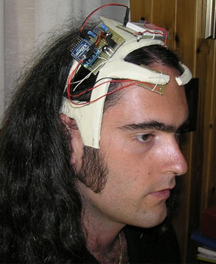
Here is a preliminary release of the headset produced before 2008/08/08
If you are interested on the making of the headset please see making rubber models
* Blood Volume pressure
First graph showing a signal acquired with the wireless sensor.
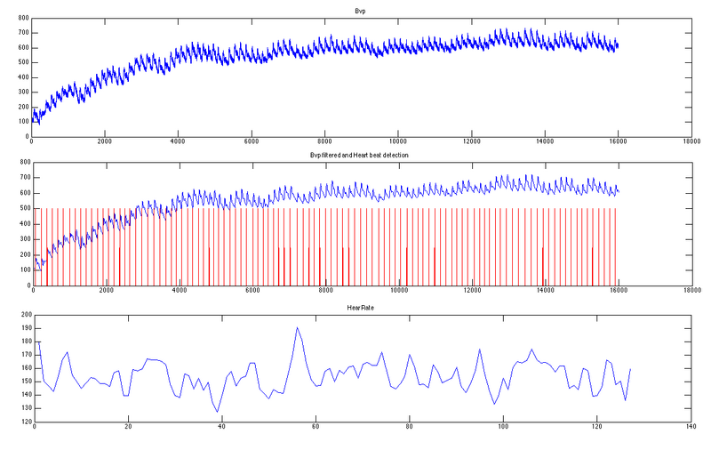
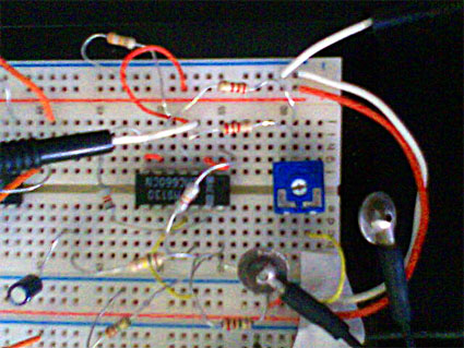
* Skin galvanic response (Sala Mirko e Alessia Cornaggia[1]) Galvanic skin response (GSR), also known as electrodermal response (EDR), psychogalvanic reflex (PGR), or skin conductance response (SCR), is a method of measuring the electrical resistance of the skin. There is a relationship between sympathetic activity and emotional arousal, although one cannot identify the specific emotion being elicited. The GSR is highly sensitive to emotions in some people. Fear, anger, startle response, orienting response and sexual feelings are all among the emotions which may produce similar GSR responses. Response of the skin to the passage of a small electric current. The ease with which the current flows between two points on the skin can be used to indicate stress. When a person is tense or emotional, the sweat glands become more active, increasing moisture on the skin; this allows the electric current to flow more readily. The response may also be used in relaxation training: information about the galvanic skin response is fed back aurally or visually to the subject who can, with practice, learn to increase or decrease sweating on the skin by learning to relax or tense muscles. We measure the galvanic skin response using two electrodes attached to the skin. The optimal placement is the palm of the hands, but we are experimenting other places like on the forehead. The circuit we are creating is the one below.
Project the device
Re-definition of the complete work
Sensors are an important part of an Affective Computing System because they provide information about the wearer's physical state or behavior. They can gather data in a continuous way without having to interrupt the user. To define in detail electronic specifications and requirements it's necessary a preliminary research/study (in literature and web) about state of art of sensor type used to monitor each type of biological signals we are interested about. In this way it's possible both understand problematics related to interaction between biological and electonical worlds and improve or re-desig existing prototype.
About Sensors:
BVP will be acquire by an IR transmitter-receiver measuring light reflected from skin (photoplethysmography). Particular attention will be put on position, geometry and power absorption of this stage.
GSR will be acquiret by a couple of electrodes forcing a low current (or voltage) and reading voltage (or current) through electrodes. Particular attention will be put on electrodes position and material. In addition is possible to foresee some problems in amplifier stage due to large range of skin resistance. Problem consist in chosing a correct amplification to overwork ADC full scale with a signal affected by little variation but huge possible range.
Temperature will be acquired by thermocouple or PTC/NTC. Slowly variable signal, possible problems with noise due to resolution required.
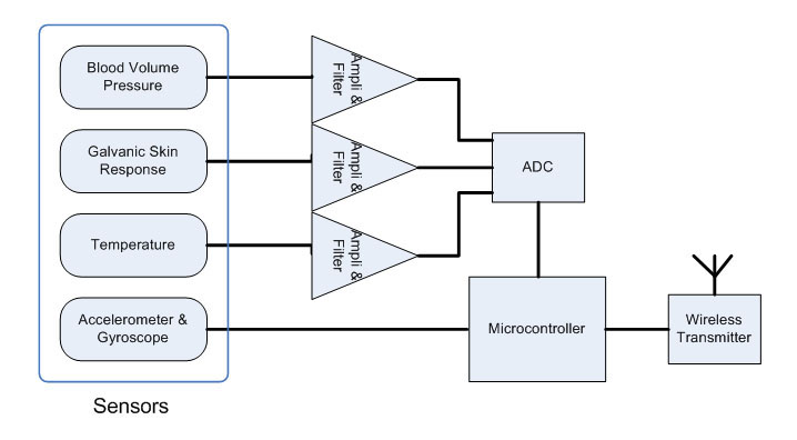
Head orientation will be acquired by an accelerometer and a gyroscope, problably integrated in the same chip. Two possibilities: analog output (need to digitalize up to six line) or digital output (like displaied in schematic block diagram).
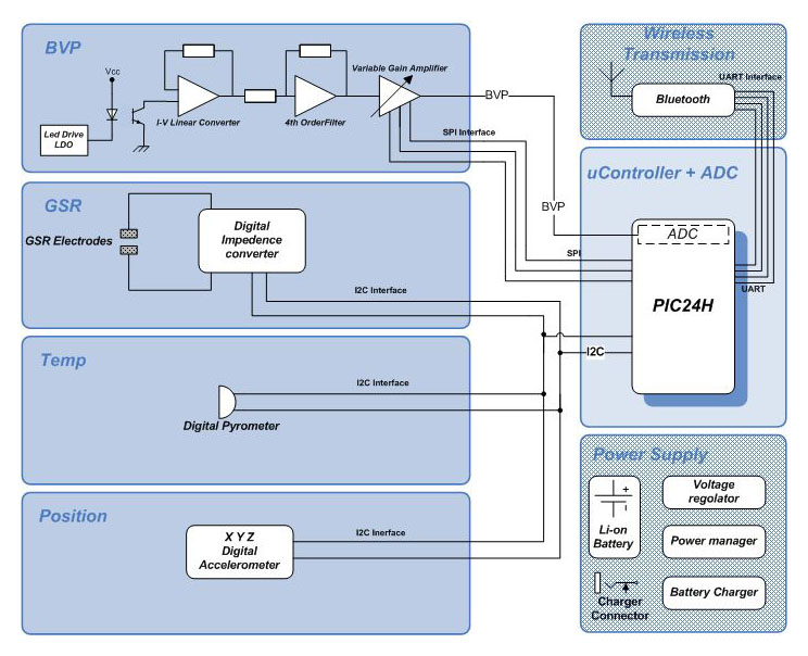
This was the preliminary simplified schematic block diagram of the complete instrumentation setup:
NOTE:

* In schematic is not present Power Supply Module: it will be based on a rechargeable Li-ion
battery. It must satisfy requirements of high efficiency, logn life and low weight.

* ADC and Microcontroller could be unified using a microcontroller with internal ADC and
internal or external multiplexer to select lines.

* Wireless section could be implemeted in Bluetooth (instead of using a XBee module like in
preliminary release) due to it's diffusion in cellular phones, notebooks, MP3 reader...
without necessity of external modules.
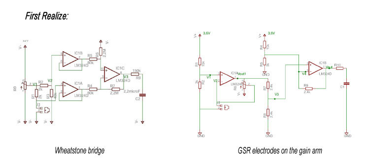
It was based on a theoretical approach to any single part. Any sensing device was designed in "conventional" way founded on analog electronic (a bridge with a NTC resisistance as sensing element, discrete IR led and some photodiode around to capture the most reflefted light as possible, GSR electrodes on the gain arm of a non-inverting amplifier...). Unfortunatly a deep analysis on signal physiology, signal transduction, noise vs required accurancy, forced us to a completely different approach implementing everywhere possible a digital interface.
Sensors Design
BVP
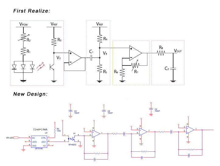
Discrete IR leds and phototransistor, used in the first realize (see fig.), had been replaced first with a single led and one or more photodiodes to optimize power consumption in case of non-planar sensor positioning. Subsequently an integrated Reflective Object Sensor was introduced, with benefits about space saving, transmitter-receiver matching and power consumption. To ensure light power stability, led is powered through a linear led drive LDO (Low Drop-Out). The choise of linear LDO is necessary to ensure no noise or spikes would be generated by charge pump systems or boost converters. In addition, the linear drive utilized requires only one external resitor to set led current and a decoupling capacitor, reducing part counts and board space occupation. The couple factor of the reflex sensors is relatively small, even in the case of good reflecting surfaces. Therefore an additional amplifier is necessary at the sensor output: classic trans-impedance amplifier used with photo-diodes and photo-transistors was introduced. This circuit features an output voltage that is a linear function of the light level on the photo-transistor. The gain is set by the feedback resistor which could be in the millions of ohms. Linear operation is achieved by operating the photo device with a fixed voltage drop across it. Trans-impedance amplifier is followed by an active fourth order band-pass filter (0.5Hz-5Hz): it's composed cascading two second order bandpass cells. In first project session only a single cell was used, but a deeper study combined with previous experiences suggests to use a 4th order filter to reduce 50Hz interference (50Hz interference produced by mains is placed only a decade after the filter pole). Filter is followed by a VGA (Variable Gain Amplifier) digitally controlled through I2C Bus that allows to optimize dinamically ADC input signal amplitude directly during acquisition session, obtaining the best performance from ADC. The resulting circuit is quite compact (led drive, reflective sensor, trans-impedence amplifier, active filter and variable-gain amplifier), doesn't require much power and represents a good mix between analog and digital approach: analog front-end with acquisition and first conditioning, and at the chain-end a digital controlled amplifier to ensure flexibility.
GSR
GSR will be acquired by a couple of electrodes forcing a low voltage and reading current through electrodes. First designs and implementations were based on literature study: best solution appears to put GSR electrodes on the gain arm of a non-inverting amplifier (see fig.) rather than using a Wheatstone bridge due to week signal produced by this solution. Putting GSR electrodes on the gain arm produces a sort of gain modulation of the constant voltage applied between electrodes but doesn't solve problems in amplifier stage due to large range of skin resistance. Problems in chosing correct amplification to overwork ADC full scale with a signal affected by little variation but huge possible range could be reduced usign a variable resistor on gain arm (for example a digital potentiometer controlled by the microcontroller), but cannot be completely removed. In addition little signals are easily deteriorated by noise. Solution is provided considering a new point of view: measure of unknown skin resistence is extremely similar to measure unknown electrical impedence with an auto-range multimeter! Solution consist in a digital Converter which combines an on-board frequency generator with a analog-to-digital converter (ADC). The resulting circuit is compact, provides a system accuracy of 0.5% and connects to microcontroller using I2C interface, ensuring an high flexibility and the possibility to modify acquisition settings after board production (through microcontroller firmware).
Temperature
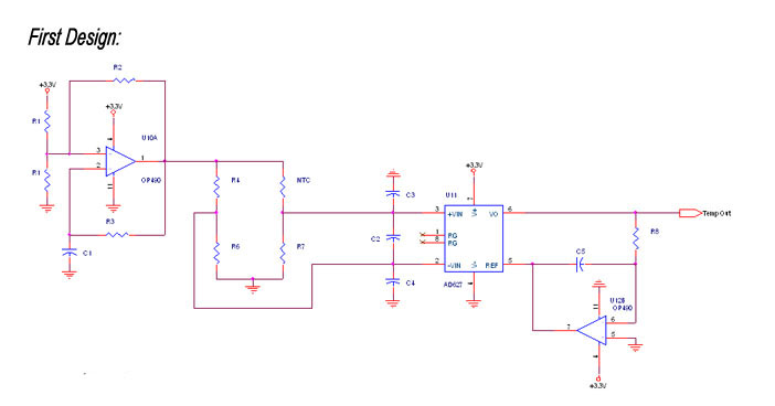
First idea was to acquire temperature by a NTC connected in a Wheatstone bridge. Trying to reduce noise, bridge was powered by an oscillator circuit with a frequency of some KHerz, to translate signal out of 1/f noise region. Bridge outputs were connected to an INA amplifier wich also implements signal filtering (see fig.). Weak signal, noise and resolution required (0.1°C) put in crisis the system. In addition other unsolved problems were the optimization of thermal and mechanical contact between sensor and body and the sensor large thermic constant. Unstable thermic contact produces unreliable measures, whereas high sensor thermic constant hampers a fast sensor response (needed to detect short peak due to emotional reactions). Possible solutions to problems of weak signal and noise arrive from digital integrated temperature sensor (for example LM35 or LM74), but these don't solve the problem of thermal contact and thermal constant. In addition none of the sensors take in consideration provides the required resolution. High resolution required, noise immunity, fast response and thermal contact immunity problems had been solved using a digital optical infrared thermometer. Small size, no external component requirements and power saving mode allow us to obtain a perfect matching between required performances and space saving.
Accelerometer
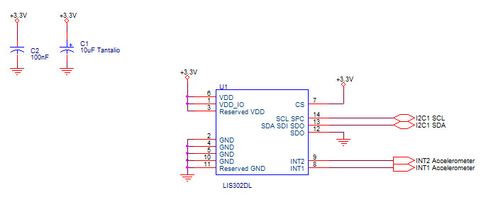
Head orientation and movements will be acquired by an accelerometer. First we think to utilize an ST Microelectronic LIS3L02AS4, due to the availability in the Lab of the evaluation board STEVAL-MKI001. It is a 3-axis ±2g/±6g linear accelerometer with 3 analog outputs, so it requires an external ADC to digitalize the three axis acceleration values. The conversion could be performed by a microcontroller with internal ADC. A fast Internet research reveled this sensor is now obsolete and out of production. The choise had been to substitute the old chip with the new one: the LIS302DL (still produced by ST Microelectronic). It's a 3-axis, ± 2g/± 8g smart digital output accelerometer with I2C/SPI digital output interface and really small package. The device is capable of measuring accelerations with an output data rate of 100 Hz or 400 Hz and the self-test capability allows the user to check the functioning of the sensor in the final application. In addition it may be configured to generate inertial wake-up/free-fall interrupt signals when a programmable acceleration threshold is crossed at least in one of the three axes. Thresholds and timing of interrupt generators are programmable by the end user on the fly. This device, providing a digital output, doesn't need signals conversion, guaranteing better noise immunity; programmable interrupts and test interface allow greater fexibility in project. In addition wery small package, only one external resistor requirement (plus baypass capacitor) reduce significantly board space requirements.
NOTE:

* In previous schematics, components phisical dimensions are not in scale.
Microcontroller
Foundamental requirements:
- High speed to ensure high data output rate even in presence of a large number af sensing elemets;
- Fast Internal ADC with multiple inputs;
- (At Least) One I2C interface;
- (At Least) One SPI interface;
- (At Least) One UART interface;
- (At Least) Three Timers;
- (At Least) Three External Interrrupts;
- Low-power consumption;
- Power supply 3.3V;
- Small package;
In addition microcontroller was chosen between Microchip PIC family devices, due to positive previous experiences and availability of software and programmer in the Lab.
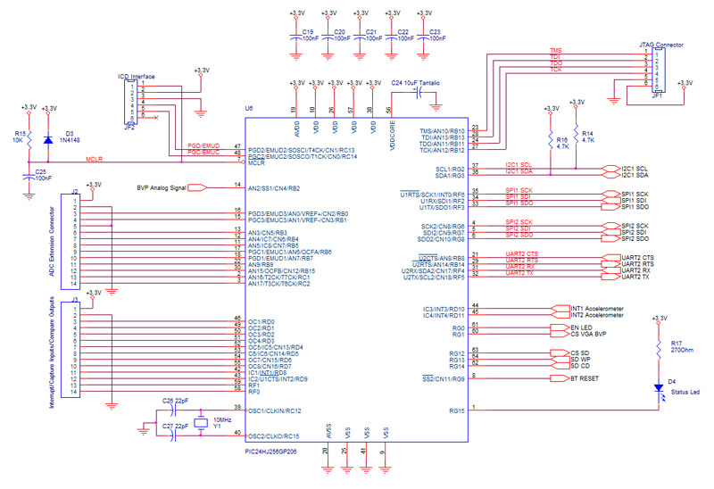
PIC24HJ256GP206 is a 16 bit microcontroller capable of 40 MIPS speed. It provides 256KB of Flash memory, 16KB of Ram, a 10-bit 1.1Msps or 12-bit 500Ksps ADC, UART, SPI and I2C interface in a 64 pin TQFP package (10mmX10mm) powerd between 3.0V and 3.6V.
Power core is provided by an internal regulator reducing parts count on the board.
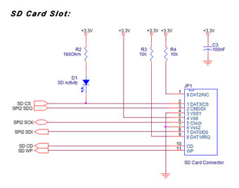
The device is able to provide at the same time one I2C interface, two SPI interface and one UART interface: another UART port shares pins with an SPI port and a second I2C port shares pins with the second UART interface. Findig a device that provides at the same time, on indipendent pins, an I2C, a SPI and an UART interface reduces considerably possible choises and suggests to chose a high performance microcontroller. At the same time, high performance solutions have a larger pin counts than standard microcontroller, but this characteristic can be used to ensure further expansibility to the system. The second SPI interface can be used to connect another "intelligent" device or a mass storage device, for example a SD (Secure Digital) card to storage acquired data (see fig.).
Input pins connected to ADC and not used at the moment could be collected to a connector for further extension modules (for example an EMG or ECG peripheral or any other analog signal interesting in a particolar application). For the same reason any other pin non used at the current stage is reported to an extension connector. To guarante maximum flexibility an further update, board provides both ICD and JTAG connections (allowing on-board programming and debugging) through a couple of indipendent dedicated connectors fully compatibles with Microchip programmers and evaluation boards.
Wireless Connection
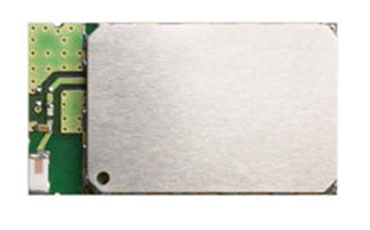
Wireless connection is based on Bluetooth 2.0+EDR (Enhanced Data Rates) module containing all the necessary elements from Bluetooth radio to antenna and a fully implemented protocol stack. Module is equipped with firmware that enables users to access Bluetooth functionality with simple ASCII commands delivered to the module over serial interface like a Bluetooth modem. The dedicated onboard microcontroller (MCU) acts as interrupt controller and event timer run the Bluetooth software stack and control the radio and host interfaces. A 16-bit reduced instruction set computer (RISC) microcontroller is used for low power consumption and efficient use of memory. Module support USB, SPI and UART interface and UART interface is used in this project to connect PIC microcontroller to wireless transmitter (see fig.).
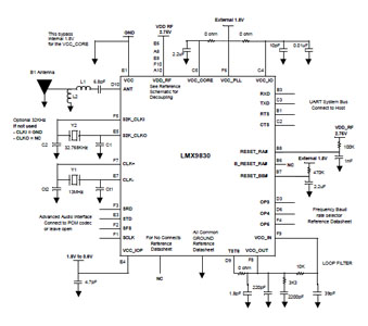
One of the most important characteristic is the high integration between all parts needed for efficent Bluetooth transmission: user interface, controller, radio circuits and antenna, all included in a low power, low size board (25.6mmx15mm) that requires a minimum number of external components. Many other bluetooth components ara available, such as LMX9830, produced by National Semiconductor. It's an extremely small device (only 6.1mm×9.1 mm), but requires a number of external components (see fig.) like oscillators, resistors, capacitors, inductors and the antenna, in addition to an high competence in radio frequency layout circuits.
Lack of experience in radio frequency circuit suggests to chose a ready-to-use module, factory optimized for best performance and easy to integrate in our board.
This is the updated simplified schematic block diagram:
Prototype realization [WIP (Work in Progress)]
Fist stage plans to realize a board using, where possible, through-hole (TH) compenents soldered on a prototyping board (100x160mm) powered from a laboratory power supply (instead of Li-on battery) and not implementing bluetooth wireless transmission. Parts not available on TH package are used with special SMD->TH adapter boards or simply fixing and soldering them to the PCB by wires.
Second stage plans to realize microcontoller firmware and test it acquiring biological signals from a patient. Firmware will be developed by subsequently steps, implementing and testing only a single peripheral at each time: only at the end single pheripheral softwares will be merged together.
Third stage will be bluetooth interface (hardware and software) implementation and integration on the board with transmission test.
Fourth stage will consider power supply optimization with battery management and recharge interface.
Finally, only after a successful full board test, the last stage will be the circuit layout design with an electronic CAD, using where possible, Surface Mount Devices (SMD) to reduce board area.
Main board
Main board include power supply regulator with led power-on indicator, PIC microcontroller (mounted on a SMD->TH adapeter board) with basic circuitry (decoupling capacitors, oscillator and programming-debugging ICD interface), a status led connected to PIC to verify basic microcontroller function, a series of connectors for add-on modules (BVP, GSR, temperature and accelerometer) and a USB PC interface not considered before.
USB interface
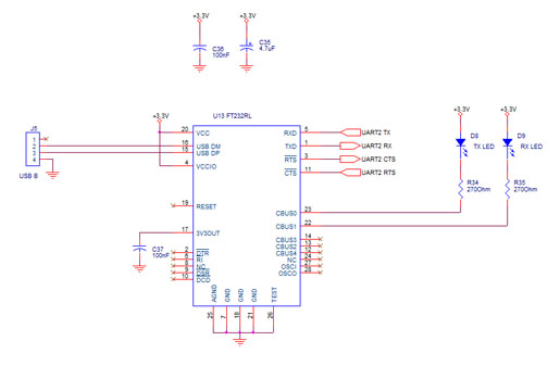
USB interface, not projected before, replaces in developing stage Bluetooth interface, allowing a direct control/communication with a PC. In this prototype PIC UART, althought being connected to Bluettoth module, is connected to a FTDI FT232RL chip. The FT232RL is the latest device to be added to FTDI’s range of USB UART interface Integrated Circuit Devices. USB to serial designs using the FT232RL have been further simplified by fully integrating the external EEPROM, clock circuit and USB resistors onto the device. The FT232RL is available in Pb-free (RoHS compliant) compact 28-Lead SSOP, so this require another SMD->TH board adapter but the circuit design is very simple, including two status led for TX and RX operations. An USB B female connector was eputated the best choise for PC connection allowing to use a simple USB printer cable.
Note that USB and Bluetooth must not be connected to the board at the same time! USB port has only a developent function.
BVP
Circuit designed for BVP acquisition (refer to previous schematic) doesn't meet the expected results. Week signal hanged by noise suggested us to re-design the circuit simplifying it and reducing the number of components. For this design also sensing element has been substitute. Instead of an integrated reflective IR sensor (SFH9202), new project use a couple af discrete IR led and photothansistor matched: SFH487 and SFH309FA. SFH487 is a very highly efficient GaAlAs infrared emitter (880 nm) and SFH309FA is a silicon NPN phototransistor especially suitable for applications of 880 nm with an high linearity. Both have a 3 mm led plastic package, are spectrum-matched and receiver is ambient-light shilded. After a series of positive test without the led driver (not used due to the really reduced mechanical dimensions), also led drive circuit was removed and replaced with a resistance connected directly to a PIC pin. This choise reduces parts count and board space required without making worse sistem performance, allowing (like led driver) to turn off the sensor led when not used to reduce power consumption.
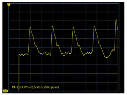
Figure show the signal measured directly on filtering stage output (TS952 pin 7) before the VGA with a Tektronix scopemeter TDS2014B. No particular triks had been used: signal has been recorded the first time circuit was assembled on a protoboard.
GSR
First approach with digital Converter resulted really hard due to some errors occurred in control software in relation with internal chip complexity and I2C bus protocol. After a start session GSR hardware acquisition interface was further simplified replacing the digital converter with a similar (same pinout and functions) one with inegrated internal oscillator.
First dataset acquired whith the correct control software and the correct data reading routine, has shown all the potentiality of this chip, providing data comparables with RAW data acquired with a bigger and very expensive professional equipement produced by ProComp.
Acceleration
Lis302DL datasheet gives a short definition of this chip as "MEMS motion sensor 3-axis - ± 2g/± 8g smart digital output “piccolo” accelerometer" and it is really very, very small for human-working. For this space saving quality this accelerometer is also use in third generation Apple i-phone. The major problem with this sensor had been to solder it to a sort of adapter to connect it to the circuit, but after that it works fine, with a good sensitivity and accuracy. Because of free fall and double click recognition at not required (at the moment) in this application, software routines for setting configuration registers and reading data resulted simplified. A usefull caracteristic of this sensor, not previously noticed, is the presence of internal pull-up resistors that allows no necessity of external I2C bus pull-up resistors, reducing space occupation and components count.
Temperature
The choice to use a digital optical infrared thermometer due to his characteristics (non contact measure, 0.02°C resolution with accuracy of ±0.1°C for medical applications version) creates a really serious supplies problem: sensor manufacture wasn't able to give us a sample and no one in Italy can sell us only a pair of theese sensors to try them. A single piece was bought from Future Electronics, ordering it via web and paying it via credit card. Fortunately the sensor, that cames directly from USA, arrived in Italy few days later the payment in excellent conditions. Problems occurred interfacing this sensor on I2C bus with other devices (GSR digital Converter and LIS302) connected. Sensor has a 2 wire serial SMBus compatible protocol: I2C bus and SMBus are popular 2-wire buses that are essentially compatible with each other, but are not the same. The buses operate at the same speed, up to 100kHz, but the I2C bus has both 400kHz and 2MHz versions. Complete compatibility between both buses is ensured only below 100kHz. Timeout and (as a consequence of timeout) minimum clock speed are the most important differences between the I2C bus and the SMBus:
I2C Bus = DC (no timeout)
SMBus = 10kHz (35mS timeout)
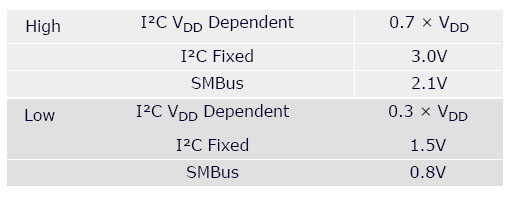
Despite differences in logic-level specifications between the two buses, generally devices can be mixed and matched with abandon. Level Specifications for the I2C Bus and the SMBus are shown below (VDD is typically expected to be between 3 volts and 5 volts):
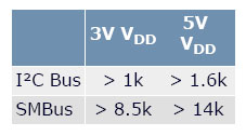
What wasn't readily evident in the discussion of voltage levels is that these levels are also specified with different currents between the buses. The SMBus specifies a minimum sink current of 100microA, and a maximum of 350microA, compared to 3mA for the I2C bus. This in turn would determine the lowest acceptable value of the pullup resistor, examples of which are shown in the table below.
In reality, it is not unusual to encounter pullup resistor values in SMBus systems, which violate this specification by being lower than recommended. A very popular range for pullup resistor values, even in some SMBus systems, seems to be 2.4k to 3.9k.
These reasons, in adition to clear ideas about close developments, suggest a general review of schematic to re-distribute microcontroller resources.
Part 6: final review [WIP (Work in Progress)]
Microcontroller
Referring to previous schematic, some chenges had been applied:
- Programmer/Debugger interface is now PGD1/EMUD1 and PGC1/EMUC1 instead of PGD1/EMUD2 and PGC1/EMUC2;
- JTAG interface had been removed;
- UART2 is no more available so UART1 has replaced UART2 as communication port;
- SPI2 is no more available so SPI1 is now used to control both VGA (Variable Gain Amplifier) and SD Storage Card;
- RG12, RG13, RG14 pins had been connected to three status led for a machine visual state detection;
- I2C1 interface is now connected to accelerometer (LIS302) and GSR Converter only;
- I2C2 interface is dedicated to temperature sensor, enabling I/O pin thresholds compliant with SMBus specification;
- Connectors for I2C, SMBus and SPI expansion modules had been added to the board;
- Test point pads had been added to the board to simplify debugging.
Data link
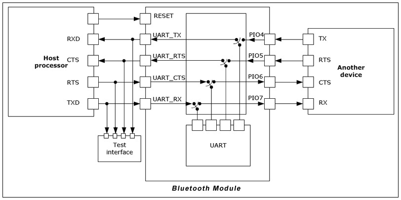
During developing stages, an USB port had replaced Bluetooth wireless transmission, allowing a direct control/communication with a PC. This interfaced, based on a FT232RL, prove to be very usefull and simple to use. The choice to use an usb port to charge internal battery, in addition to availability of a UART multiplexer inside the Bluetooth, suggest to implement both USB and Bluetooth interface.
That's the Bluetooth internal UART multiplexer schematic:
Battery Charge & MonitorPower On
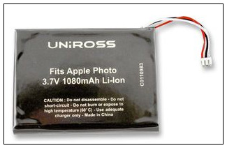
Device is powered by a single cell Li-on battery (3.7V, 1080mAh): this is the same unit used in IPod(TM) from Apple.
Battery charge is executed by a Maxim's device: it is a really compact single-cell lithium-ion (Li+) battery charger that can be powered directly from a USB port or from an external supply up to 6.5V. It has a 0.5% overall battery regulation voltage accuracy to allow maximum utilization of the battery capacity. The charger uses an internal FET to deliver up to 500mA charging current to the battery. The device can be configured for either a 4.1V or 4.2V battery, using the SELV input. The SELI input sets the charge current to either 100mA or 500mA. An open-drain output indicates charge status. It has preconditioning that soft-starts a near-dead battery cell before charging. Other safety features include continuous monitoring of voltage and current and initial checking for fault conditions before charging.
White battery wire (see photo) is connected to internal NTC thermistor (10KOhm@+25°C). In this way it's posible to implement an over/under charge temperature detector using a couple af operational amplifier as comparator. With a resistence network it had been possible to set an upper temperature threshold of 47.5°C (corresponding to 3.97K NTC value) and a down thresold of 2.5°C (corresponding to 28.7K NTC value). Out of this range comparators output go low disabling battery charger. This function allows to prevent battery demage or explosion during charge.
Battery voltage monitor is hardware implemented by a CMOS micropower voltage detector that warn microprocessors/microcontroller of power failures. It contains a comparator, a 1.5V bandgap reference, and an open-drain n-channel output driver. Two external resistors are used in conjunction with the internal reference to set the trip voltage to the desired level. A hysteresis output is also included, allowing the user to apply positive feedback for noise-free output switching. Using a couple of these device is possible to set two treshold: one for low battery and another for end battery detection. Low battery detection allow communicate the user battery level; end battery detection allow microprocessor shut down the device before battery voltage fall down under 3.4V that is the minimun input voltage allowed by linear regulator MCP1700. If battery level fall down under 3.4V, MCP1700 is not able to guarantee line regulation.
Power On & Selection
Power-up and shut-down were implemented using a Maxim's MAX16054 connected with an ADG801 by Analog Device. MAX16054 is a pushbutton on/off controller with a single switch debouncer and built-in latch. It accepts a noisy input from a mechanical switch and produces a clean latched digital output after a factory-fixed qualification delay. The state of the output changes only when triggered by the falling edge of the debounced switch input; the output remains unchanged on the rising edge of the input.An asynchronous CLEAR input allows an external signal to force the output flip-flop low. ADG801 is a monolithic CMOS, single-pole, single throw (SPST), normally open (NO) switch with on resistance of less than 0.4Ohm. This switch conducts equally well in both directions when on.
MicroSD Storage Card
RTC
Students that have worked on the project
- Mattia Colombo (Blood Volume Pressure sensor)
- Alessia Cornaggia (Galvanic skin response sensor)
- Sala Mirko (Galvanic skin response sensor)
Laboratory work and risk analysis
Laboratory work for this project will be mainly performed at AIRLab/Lambrate. It will include electrical and electronic activity. Potentially risky activities are the following:
- Use of mechanical tools. Standard safety measures described in Safety norms will be followed.
- Use of soldering iron. Standard safety measures described in Safety norms will be followed.
- Use of high-voltage circuits. Special gloves and a current limiter will be used. Standard safety measures described in Safety norms will be followed.
Detailed Information and Schematics available in the Discussion page.
